When you purchase through links on our site, we may earn an affiliate commission.Heres how it works.
This innovation could shrink rig sizes, improve energy efficiency, and reduce manufacturing costs.
The GaN wafers unique crystal structure is key to its dual functionality.
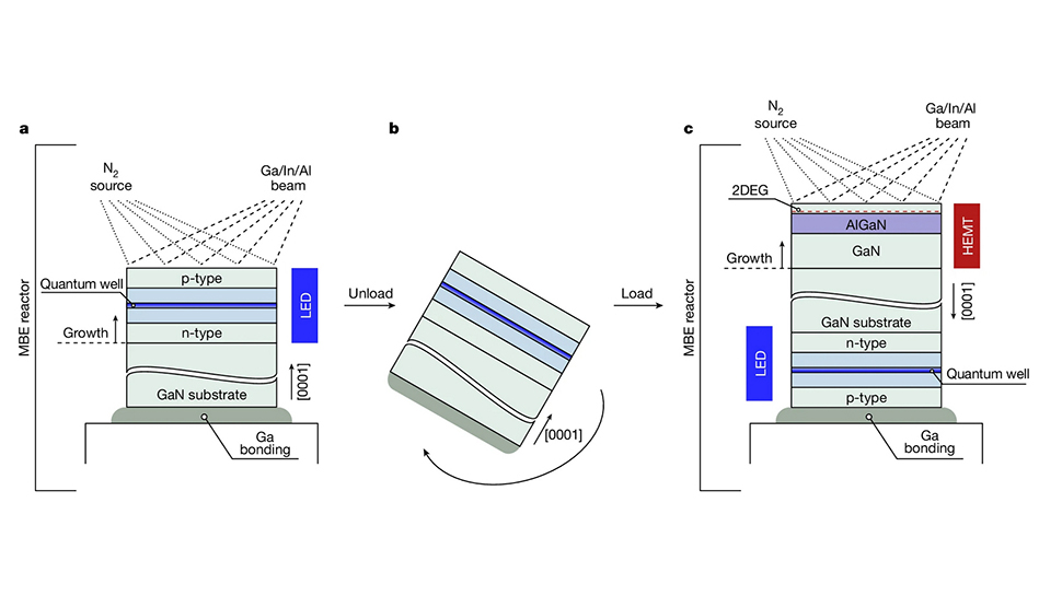
The grey arrows indicate the chronological order of the growth procedure.a, Ga bonding of the GaN substrate and MBE growth of the (In,Ga,Al)N LED along the metal-polar direction.b, Unloading, cleaning, flipping, Ga bonding and reloading of the sample.c, MBE growth of the GaN/AlGaN HEMT along the N-polar direction.
Each side of the wafer has different properties, similar to how the poles of a magnet differ.
Traditional silicon wafers are cubic, making both sides nearly identical, which prevents such a design.
This advancement could significantly impact display manufacturing, potentially making LED displays cheaper and more compact.
The technologys potential goes even further.
A good analogy is the iPhone, explained Debdeep Jena.
It is, of course, a phone, but it is so many other things.
Its a calculator, its a map, it lets you check the internet.
So theres a bit of a convergence aspect of it.
This breakthrough could reshape how semiconductor devices are designed and utilized.
